- Water Testing Meters
- Anemometer
- Length & Distance Meter
- Multimeter & Clamp Meter
- Light and Sound Meter
- Slide Calipers & Screw Gauge
- Thermometer & Hygrometer
- Milk Testing Meters
- Paper, Grain & Wood Testers
- Stopwatch & Timers
- Soil Testing Meters
- Refractometers & Analyzer
- Magnetic Compass
- Tachometer & Megger
- Thickness & Dia-Meters
- Other Meter And Accessories
4049 Buffer IC
৳ 30.00
- 4049 Buffer IC
- Voltage Rating:-0.5V to20V
- DC Input Current, Any One Input:±10mA
- Temperature Range: -55°C to 125°C
SKU:
38341
Category: Electronic Components
Tags: Electronics Lab Equipment in Bangladesh, General ICs, IC, Integrated Circuits
Description
The CD4049UB and CD4050B or 4049 Buffer IC devices are inverting and non-inverting hex buffers, respectively, and feature logic-level conversion using only one supply voltage (VCC). The input-signal high level (VIH) can exceed the VCC supply voltage when these devices are used for logic-level conversions. These devices are intended for use as CMOS to DTL/TTL converters and can drive directly two DTL/TTL loads. (VCC = 5V, VOL £ 0.4V, and IOL ³ 3.3mA.)The CD4049UB and CD4050B are designated as replacements for CD4009UB and CD4010B, respectively. Because the CD4049UB and CD4050B require only one power supply, they are preferred over the CD4009UB and CD4010B and should be used in place of the CD4009UB and CD4010B in all inverter, current driver, or logic-level conversion applications. In these applications, the CD4049UB and CD4050B are pin-compatible with the CD4009UB and CD4010B, respectively, and can be substituted for these devices in existing as well as in new designs. Terminal No. 16 is not connected internally to the CD4049UB or CD4050B; therefore, connection to this terminal is of no consequence to circuit operation. For applications not requiring high sink current or voltage conversion, the CD4069UB Hex Inverter is recommended.
Features of the 4049 Buffer IC
- CD4049UB Inverting
- CD4050B Non-Inverting
- 4049 Buffer IC
- High Sink Current for Driving 2 TTL Loads
- High-To-Low Level Logic Conversion
- 100% Tested for Quiescent Current at 20V
- Maximum Input Current of 1mA at 18V Over Full Package Temperature Range; 100nA at 18V and 25oC
- 5V, 10V and 15V Parametric Ratings Applications
- CMOS to DTL/TTL Hex Converter
- CMOS Current “Sink” or “Source” Driver
- CMOS High-To-Low Logic Level Converter
- Voltage Rating:-0.5V to20V
- DC Input Current, Any One Input:±10mA
- Temperature Range: -55°C to 125°C
- Made in China
Reviews (0)
Only logged in customers who have purchased this product may leave a review.
About brand
Labtex is a seller, supplier, and stockist of Chinese-branded and non-branded lab equipment, scientific instruments, chemicals, reagents, microscopes, telescopes, medical devices, etc., in Bangladesh. Labtex always tries to sell the original products through the website and direct sales.
Shipping & Delivery
🚚 Delivery within 1–3 working days in Dhaka City and 3–5 working days across Bangladesh. Shop confidently from the largest scientific store in Bangladesh with 2200+ products. Our Delivery Partners: Pathao, SteadFast, Sundarbon, etc.
Related products
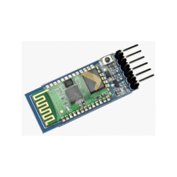
Arduino Bluetooth Module HC-05
3 in stock
IC 7408 / 74HC08 Quad 2-input AND Gate
18 in stock


Reviews
There are no reviews yet.